———————————- UPDATE ————————————–
For a ADC Input Frontend with Auto-range capabilities in the 0-40V Input range take a look also at the new ADC Input related article
—————————————————————————————
——————————— NEW UPADTE —————————————-
Added also a new example for a 0-5V input range with Voltage divider and LSB calculation, “the easy way”: ESP8266 internal ADC 2 – the easy way example
Added also a new example for a 0-5V input range with Voltage divider and LSB calculation, “the easy way”: ESP8266 internal ADC 2 – the easy way example
After talking in the previous article about DAC (Digital to analog conversion) let’s take a look also to the ADC (Analog to Digital Conversion) process story.
What is the purpose of an ADC ?
The ADC translates an analog input signal to a digital output value representing the size of the input relative to a reference.
The ADC translates an analog input signal to a digital output value representing the size of the input relative to a reference.
One of the good news about is that ESP8266 has an ADC inside and at least ESP-07, ESP-12, Olimex MOD-WIFI-ESP8266-DEV modules have the ADC Pin available.
 |
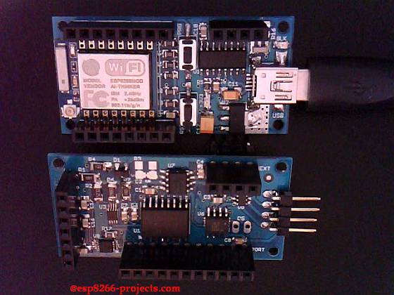
| ESP8266 – ESP-07 Module |
 |
| Olimex MOD-WIFI-ESP8266-DEV |
Some not so good news about ESP8266 internal ADC, at least until now:
- Documentation available it’s at a very poor level. More like a leaflet combined with a marketing presentation. If you were able to find anything more than this one please feel free to share.
- Only one ADC, one analog input pin, resolution probably determined by the ESP8266 community as been a 10 Bit one thru trial and error or some internal data leakage and has a not so clear range from 0 to about 1V. No other technical specifications. None. Engineering fun 🙂
- Should I ask about the voltage reference? 🙂
So, the legitimate Question arrived: it is any good for anything or just a fancy added function for marketing purposes ? Well…will see below
The first simple application that has come in my mind was to use the new builded Li-ion Battery Module to power up ESP8266 module and in the same time to read the Li-ion Cell voltage thru a long period of time. A voltage logger for the Li-ion Cell if you want. 10 Bits resolution must be enough for the purpose of the experiment, to see some trending data for the Li-ion Cell.
What we will need:
- CBDB Board
- USB adapter (take a look on Part 1 for details how to connect them together)
- Battery pack
- Voltage Divider as below
General considerations :
As maximum voltage input is expected to be 1V only and because our Li-ion Cell fully charged voltage goes up to 4.2-4.3V it’s obviously that we need to find a way to “translate” the voltage domain between 0-4.3V to 0-1V. They are many different techniques available for doing that but the easiest one and the one that we will use here is the Resistive Voltage Divider (RVD).
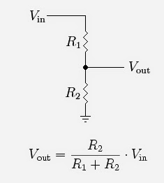
A RVD (also known as a potential divider) is a passive linear circuit that produces an output voltage (Vout) that is a fraction of its input voltage (Vin). Voltage division is the result of distributing the input voltage among the components of the divider.
We will use for our project the simpler example of a voltage divider: two resistors connected in series, with the input voltage applied across the resistor pair and the output voltage emerging from the connection between them.
 |
|
| Voltage divider schematic and Vout formula |
The result:
 |
| Voltage divider |
Few observations about:
- use high quality resistors, 1% or less with as small as possible ppm/C. In this case were used metal film resistors, 1%, 50ppm/C. Try to avoid carbon ones.
- avoid long wires that can produce itself a voltage drop due to internal resistance. For a quick explanation and calculation take a look here and for PCB traces here
- yes, I know, pedants might say breadboard is not a good idea for something like that but believe me, in this case, for a quick test, will make no difference. It’s a 10 Bit ADC and we are doing trending measurement.
Let’s find out what resistor values we will need for our RVD:
- Vinmax = 4.3 V
- Voutmax = VADCin_max = 1V
- Vout=Vin*R2/(R1+R2)
From the resistor ratio calculation choosed values are: R1=33K and R2=10k. You can choose also other values as long as you keep accurate the ratio between, better go upper that that. 330k and 100k should give the same result for example.
Software implementation
For programming CBDB Board and uploading the driver and the software we will continue to use the LuaUploader as before.
We will implement 3 different type of ADC Read functions, to see if any notable difference:
1. READ_ADC function:
        function readADC()                 -- simple read adc function
           ad = 0
          ad=ad+adc.read(0)*4/978   -- calibrate it based on your voltage divider AND Vref!
          print(ad)
         return ad
     end
2. READ_AVG ADC function:
       function readADC_avg()                 -- read 10 consecutive values and calculate average.
           ad1 = 0
           i=0
           while (i<10) do
                ad1=ad1+adc.read(0)*4/978 --calibrate based on your voltage divider AND Vref!
                --print(ad1)
                i=i+1
           end
           ad1 = ad1/10
           print(ad1)
           return ad1
      end
2. READ_ DCM function:
As probably Read_ADC() and Read_AVG() are pretty straigh forward things I will not insist on them. Read_DCM() function it’s a little bit special, as is using a special technique called oversampling and decimation.
The theory behind oversampling and decimation is rather complex, but using the method is fairly easy. The technique requires a higher amount of samples. These extra samples can be achieved by oversampling the signal. For each additional bit of resolution, n, the signal must be oversampled four times. To get the best possible representation of a analog input signal, it is necessary to oversample the signal this much, because a larger amount of samples will give a better representation of the input signal, when averaged.
That means that in our case if we want to increase resolution from 10 to 12 bit we will need to take 16 samples.
Another requirement to make this method work properly is that the signal-component of interest should not vary during a conversion. However another criteria for a successful enhancement of the resolution is that the input signal has to vary when sampled. This may look like a contradiction, but in this case variation means just a few LSB. The variation should be seen as the noise-component of the signal. When oversampling a signal, there should be noise present to satisfy this demand of small variations in the signal.
As a conclusion from other ADC related work, IF Read_ADC() will give us very good and accurate results Read_DCM() will go bad and vice-versa.
      function readADC_dcm()
         ad2 = 0
         i=0
         while (i<16) do
               ad2=ad2+adc.read(0)
               --print(ad2)
               i=i+1
          end
          ad2 = bit.rshift(ad2, 2)
          ad2= ad2*0.001020880 -- 12Bit step value-calibrate based on your voltage divider AND Vref!
          print(ad2)
          return ad2
     end
Some first time run results:
Adding a Web interface it’s an easy task :
 srv=net.createServer(net.TCP)
  srv:listen(80,
     function(conn)
           conn:on("receive",function(conn,payload)
            --print(payload)
           conn:send("HTTP/1.1 200 OK\n\n")
           conn:send("<META HTTP-EQUIV=\"REFRESH\" CONTENT=\"5\">")
           conn:send("<html><title>LOG Server - ESP8266</title><body>")
           conn:send("<h1>Data Logger Server - ESP8266</h1><BR>")
           conn:send("Voltage    :<B><font color=red size=4>"..string.format("%g",ad)..
                             " V</font></b><br>")
           conn:send("Voltage AVG:<B><font color=red size=4>"..string.format("%g",ad1)..
                             " V</font></b><br>")
           conn:send("Voltage DCM:<B><font color=red size=4>"..string.format("%g",ad2)..
                             " V</font></b><br>")
           conn:send("<BR><BR><BR>Node.HEAP     : <b>" .. node.heap() .. "</b><BR>")
           conn:send("IP ADDR    :<b>".. wifi.sta.getip() .. "</b><BR>")
           conn:send("TMR.NOW    :<b>" .. tmr.now() .. "</b><BR<BR><BR>")
           conn:send("</html></body>")
           conn:on("sent",function(conn) conn:close() end)
           conn = nil
      end)
end)
Test Video:
2 Comments
xavier · August 15, 2017 at 6:20 pm
Hi
I don’t understand your calibration: ad=ad+adc.read(0)*4/978
I expected formula like: ad=adc.read(0)*(33K+10K)/10K
Where is my mistake?
Where are coming from those magic numbers: 4 and 978?
esp8265_wp · August 18, 2017 at 7:48 am
Hi xavier,
It is related with the voltage divder multiplication factor,maximum ESP8266 ADC input voltage as I found it by direct measurement,Vref, etc.
If it looks to convoluted, please take a look at the new example for a 0-5V input range with Voltage divider and LSB calculation, “the easy way”:)
http://esp8266-projects.org/2016/08/esp8266-internal-adc-2-the-easy-way-example/
Happy breadboarding,
TJ.