In this part we will talk a bit about the nEXT Bus I²C protocol and we will start also a longer, multi-part discussion about testing procedures and software programming for the AN1 Board devices and functions (I/O Expansion port, Temperature, ADC, DAC, Voltage measurements,etc.
Previous related Articles:
- New ESP8266 DevBoard – CBDB nEXT EVO – General presentation, schematics, PCB, etc
- Part 2 – ESP8266 DevBoard – CBDB nEXT EVO – Firmware upload
- SSD1306 OLED Display for ESP8266 nEXT EVO Board
- ESP8266 nEXT EVO – Analog Extension Board – Part 1 – General view, schematics, PCB, etc
————————————————————————————————————————–
For any new CBDB orders/requests please feel free to use as usual:
tech at esp8266-projects.com.
ESP8266 nEXT Evo bare PCB has also been made available directly at Dirty PCBs, our preferred PCB House for experimenting (**):
http://dirtypcbs.com/view.php?share=9699&accesskey=91d782fd4a10943fd36ecc371c7ff2cd
(**) – Actually you have there 2 Boards for the price of one, a ESP8266 nEXT Evo together with a AN1 nEXT Analog Extension Board that brings you a 18Bit ADC (autoscale 0-40V input!), 4x12Bit DAC, Precison Temperature measurement, 8bit I/O port, etc.
————————————————————————————————————————-
For today topic let’s have first a brief look at the nEXT bus protocol: I²C
What is I²C?
I²C (Inter-Integrated Circuit), pronounced I-squared-C, is a multi-master, multi-slave, single-ended, two-wired serial bus – SDA (data line) and SCL (clock line) – invented by Philips Semiconductor (now NXP Semiconductors). It is typically used for attaching lower-speed peripheral ICs to processors and microcontrollers.
Features of the I2C-bus:
- Only two bus lines are required; a serial data line (SDA) and a serial clock line (SCL).
- Each device connected to the bus is software addressable by a unique address and simple master/slave relationships exist at all times; masters can operate as master-transmitters or as master-receivers.
- It is a true multi-master bus including collision detection and arbitration to prevent data corruption if two or more masters simultaneously initiate data transfer.
- Serial, 8-bit oriented, bidirectional data transfers can be made at up to 100 kbit/s in the Standard-mode, up to 400 kbit/s in the Fast-mode, up to 1 Mbit/s in Fast-mode Plus, or up to 3.4 Mbit/s in the High-speed mode.
- Serial, 8-bit oriented, unidirectional data transfers up to 5 Mbit/s in Ultra Fast-mode
- On-chip filtering rejects spikes on the bus data line to preserve data integrity.
- The number of ICs that can be connected to the same bus is limited only by a maximum bus capacitance. More capacitance may be allowed under some conditions.
SDA and SCL signals
Both SDA and SCL are bidirectional lines, connected to a positive supply voltage via a current-source or pull-up resistor:
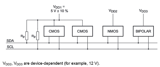
When the bus is free, both lines are HIGH. The output stages of devices connected to the bus must have an open-drain or open-collector to perform the wired-AND function. Data on the I²C-bus can be transferred at rates of up to 100 kbit/s in the Standard-mode, up to 400 kbit/s in the Fast-mode, up to 1 Mbit/s in Fast-mode Plus, or up to 3.4 Mbit/s in the High-speed mode. The bus capacitance limits the number of interfaces connected to the bus.
For a single master application, the master’s SCL output can be a push-pull driver design if there are no devices on the bus which would stretch the clock.
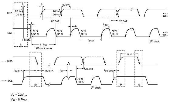
SDA and SCL logic levels
Due to the variety of different technology devices (CMOS, NMOS, bipolar) that can be connected to the I²C-bus, the levels of the logical ‘0’ (LOW) and ‘1’ (HIGH) are not fixed and depend on the associated level of VDD.
Input reference levels are set as 30 % and 70 % of VDD; VIL is 0.3VDD and VIH is 0.7VDD.
 |
| Timing Diagram for F/S-mode devices on the I²C-bus |
Some legacy device input levels were fixed at VIL= 1.5 V and VIH= 3.0 V, but all new devices require this 30 %/70 % specification.
For a more deep and extensive I²C protocol undestanding ( Data Validity, START and STOP conditions, Byte format, Acknowledge (ACK) and Not Acknowledge (NACK), Clock synchronisation, etc,etc please take a look at the official NXP I²C Protocol datasheet. I²C protocol it is quite a serious separate topic to discuss :).
Before going further with our main topic I will insist only one one more thing, as it looks it creates a lot of confusion sometime:
The slave address and R/W Bit (7 bit mode) !
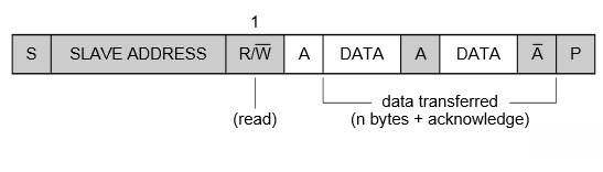
Data transfers follow the format shown in the picture below:
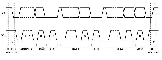 |
| A full data transfer |
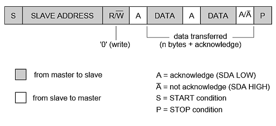
After the START condition (S), a slave address is sent. This address is seven bits long followed by an eighth bit which is a data direction bit (R/W) — a ‘zero’ indicates a transmission (WRITE), a ‘one’ indicates a request for data (READ):
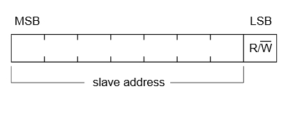 |
| The first byte after the START procedure |
A data transfer is always terminated by a STOP condition (P) generated by the master.
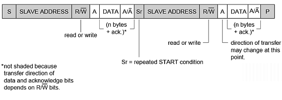
However, if a master still wishes to communicate on the bus, it can generate a repeated START condition (Sr) and address another slave without first generating a STOP condition. Various combinations of read/write formats are then possible within such a transfer:
- Master-transmitter transmits to slave-receiver. The transfer direction is not changed and the slave receiver acknowledges each byte:
- Master reads slave immediately after first byte. At the moment of the first acknowledge, the master-transmitter becomes a master-receiver and the slave-receiver becomes a slave-transmitter. This first acknowledge is still generated by the slave. The master generates subsequent acknowledges. The STOP condition is generated by the master, which sends a not-acknowledge (A) just before the STOP condition:
- Combined format. During a change of direction within a transfer, the START condition and the slave address are both repeated, but with the R/W bit reversed. If a master-receiver sends a repeated START condition, it sends a not-acknowledge (A) just before the repeated START condition:
Now, after a very brief (very!) I²C protocol presentation, let’s go back to our Analog Extension Board:
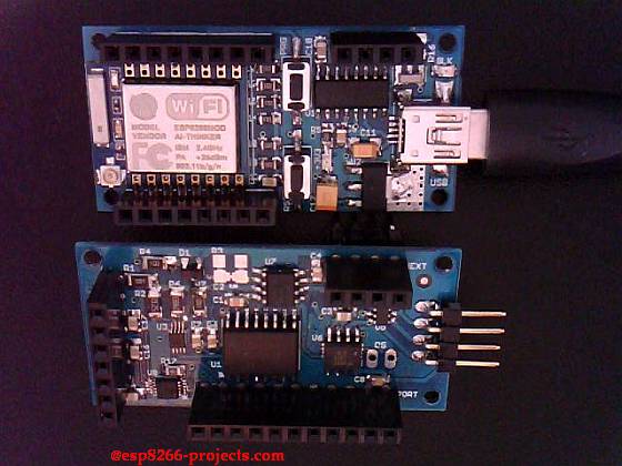 |
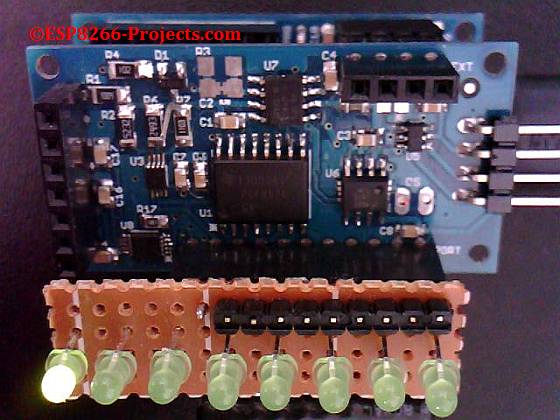
| ESP8266 nEXT EVO + AN-1 Boards |
First thing that we want to do, after the AN-1 Board is properly soldered, cleaned, visual inspection OK, etc, will be to tests it and validate it as a proper working Board.
What we will need:
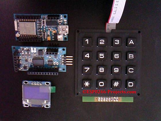
- ESP8266 nEXT EVO Board
- ESP8266 nEXT EVO – Analog Extension Board – AN1
- For programming and uploading the driver and the software we will continue to use the LuaUploader as before.
Connection with the ESP8266 nEXT EVO Board is very easy, as Analog Extension Board – AN1 connector is fully compatible with the nEXT connector. Depending on how to you choose you socket type, you can install it on TOP or Bottom of the ESP8266 nEXT EVO Board :
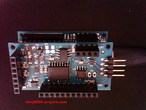 |
| ESP8266 nEXT EVO Board + Analog Extension Board AN1 |
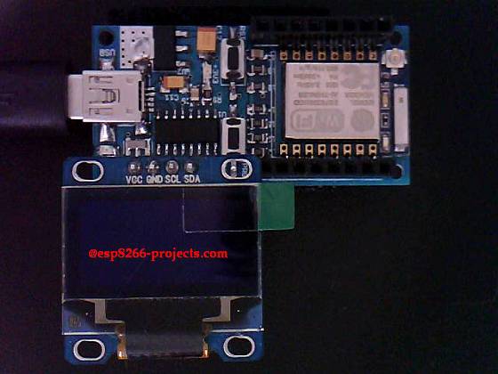
And, if you want, you can continue stacking them on the nEXT Bus, with a SSD1306 OLED Display, for example:
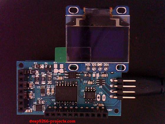 |
| ESP8266 nEXT EVO + AN1 + SSD1306 OLED Display |
Software implementation
By default, on the AN-1 Board you should have the following available devices:
- PCF8574 8Bit I/O Extension port – at address 0x20
- LM75 Temperature sensor – at address 0x48
- MCP4728 – 4x12Bit DAC – at address 0x60
- MCP3421 – 18Bit ADC – at address 0x68
When also connected, the SSD1306 OLED Display will be available at 0x3C
A fist step in testing the AN-1 available functions and devices will be to scan the nEXT I²C Bus and see if all the existing ones are alive and responding to the I²C Master requests. Also will list any new added devices, if alive.
1. Find device function
 function find_dev(i2c_id, dev_addr)
     i2c.start(i2c_id)
     c=i2c.address(i2c_id, dev_addr ,i2c.TRANSMITTER)
     i2c.stop(i2c_id)
     return c
end
2. Scan Bus for devices function
 function scanbus()
     i2c.setup(id,sda,scl,i2c.SLOW)
     for i=1,127 do
        if find_dev(id, i)==true then
             if i==32 then
             print("- PCF8574 8Bit I/O Extension port - found at address 0x"..string.format("%02X",i).." -> "..i)
             else
             if i==72 then
             print("- LM75 Temperature sensor         - found at address 0x"..string.format("%02X",i).." -> "..i)
             else
             if i==96 then
             print("- MCP4728 - 4x12Bit DAC           - found at address 0x"..string.format("%02X",i).." -> "..i)
             else
             if i==104 then
             print("- MCP3421 - 18Bit ADC             - found at address 0x"..string.format("%02X",i).." -> "..i)
             else
             if i==60 then
             print("- SSD1306 OLED Display            - found at address 0x"..string.format("%02X",i).." -> "..i)
             else
             print("- NEW UNREGISTERED DEVICE         - found at address 0x"..string.format("%02X",i).." -> "..i)
             end
           end
         end
        end
        end
        end
        tmr.wdclr()
    end
 end
3. MAIN Scanbus Program
id=0
sda=2
scl=1
scanbus()